Pharma 4.0 and the Semiconductor Industry
It has been almost 15 years since the creation of the 21st Century cGMP initiative by the Food and Drug Administration (FDA). The main goal of this initiative was to encourage the adoption of innovative manufacturing technologies within the pharmaceutical industry.1 Unfortunately, a mixture of cultural resistance and regulatory uncertainty has made the biopharma journey towards innovation slow and frustrating to some, especially to the Process Analytical Technologies (PAT) aficionados. Nonetheless, excitement has resurged during the last couple of years. This is in part thanks to several industrial factors and trends such as the FDA’s approval of two small molecule continuous manufacturing applications, the embrace of PAT in biologicals and the world-wide excitement around big data analytics.2-6 This later trend, and inevitable change, is expected to promote an exponential cultural transformation within an industry that is well known to be technologically conservative. The new generation of biopharma process engineers and leaders were academically and socially developed in an era of smart devices, networked systems and on-demand data visualization and analytics, thus the Industry 4.0 concept is just an extension of their daily routine rather than an industrial paradigm shift. Also, the trend towards smart manufacturing and the government efforts to promote cutting edge innovation has resulted in collaborative efforts between academia, government and industry to promote cyber-physical systems to enable more efficient and competitive manufacturing practices.7,8
Even though it is true that the pharmaceutical industry is heading in the right direction and that there are multiple groups acting as change agents by demonstrating the value of advanced measurements, advanced data analytics and advanced controls,4,5,9 there is still significant work to be done. This is particularly true in the areas of Information Technology (IT) system integration and process automation, which are critical to enhance process performance metrics and overall Operational Excellence (OpEx). The level of process improvements that can be gained by adopting newer manufacturing technologies is evident when benchmarking biopharma with other high tech Silicon Valley industries which have been forced to innovate in order to guarantee their survival in the markets. One industry, besides automotive, which is often cited as a “role model” of manufacturing performance is semiconductors.10,11Table 1 shows a comparison between pharma and semiconductor performance metrics. In this comparison we can see significant differences in performance metric values, with semiconductor manufacturing operating at higher process capabilities and Overall Equipment Effectiveness or OEE.12
Table 1. Comparison between two critical semiconductor and pharma manufacturing performance metrics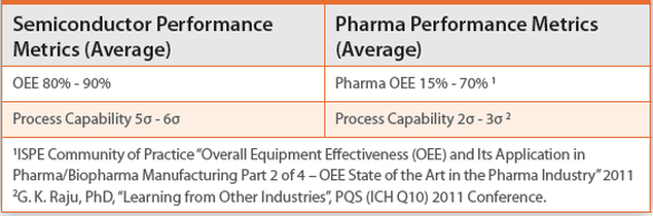
When comparing performance metrics values between these two industries, it is impossible not to wonder why the marked difference between them and what can pharma leverage from Silicon Valley to increase the efficiency and effectiveness of their processes while maintaining and/or even improving quality compliance. In order to answer some of these questions, it is important to understand the complexities faced by the semiconductor manufacturing sector and their journey towards quality, effectiveness, efficiency and cutting edge innovation.
Semiconductor Manufacturing
During the semiconductor chip manufacturing process, a silicon wafer is transformed into a grid of silicon chips.13 Each silicon chip or “die” is manufactured to have identical layers of complex circuitry within the wafer14 ( see Figure 1).
 Figure 1. Silicon wafer after patterning, each silicon chip or “die” is manufactured to have identical layers of complex circuitry within the wafer. Picture courtesy of Applied Materials.
Chip manufacturing processes consist of a series of film depositions and etching operations and usually have hundreds of controlled steps and thousands of potential failure points. Furthermore, the spatial resolution and precision needed from the associated manufacturing measurement and control equipment could be at the nano and angstrom level.15 These tight quality and process control requirements, which are driven by market demands, have forced the semiconductor industry to develop and adopt sophisticated measurement, automation and control strategies which include advanced sensing and diagnostics, advanced process control (APC), precise robotics and machine learning. Developing and adopting advanced technologies has allowed semiconductor factories to meet quality and market demands while staying profitable. Advanced automation has also allowed minimizing unwanted human to process interaction. This in turn has reduced human error, operator-to-operator variability and human related contamination risk. Reducing human to process interaction has also minimized human exposure to the hazardous chemicals that are used during semiconductor processing, thus increasing operator’s safety.
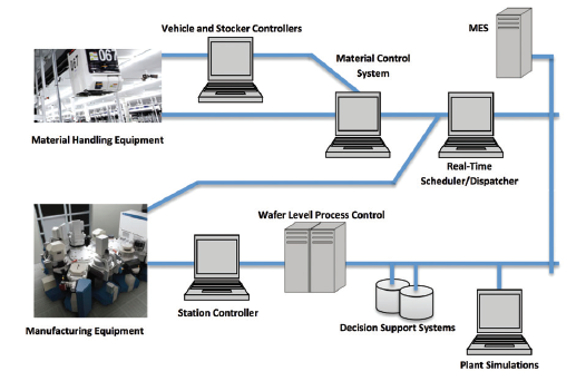 Figure 2. Integrated semiconductor automation schematic (adapted from “Handbook of Semiconductor Manufacturing Technology” Second Edition). In semiconductor production, Material Control Systems (MCS) initiate and coordinate the movement of materials by using intelligent equipment and optimizers. Manufacturing automation systems are also networked to the ERP to incorporate further business intelligence into the production.
Advanced Manufacturing Practices in the Semiconductor Industry
Some of the automation, control and advanced sensing strategies commonly found in semiconductor factories are real-time optimizers for scheduling and dispatching, model-based APC, multivariate diagnostics, predictive maintenance and soft sensing of unmeasured or unmeasurable process variables and product quality. This last application is known within the semiconductor industry as “virtual metrology.”16-18 In a semiconductor plant, real-time optimizers are not only utilized to optimize the process flow, but also to optimize the entire business operation.19 For example, at semiconductor plants ISA-95 Level 1 and Level 2 process and automation information are vertically networked to the Enterprise Resource Planner (ERP) to optimize scheduling and dispatching in real-time using heuristic and/or genetic logic.20-22 This allows the process to compensate for unscheduled downtime, prioritize production based on ERP directives and lower performing assets in order to produce at, or under, Takt time. Figure 1 depicts a high level schematic of process integration commonly found in semiconductor manufacturing plants. The integration of systems allows orchestrating the process to reduce scrap, reduce human error and increase output.
Advanced Dispatching and Scheduling
Intelligent dispatching and scheduling has enabled semiconductor manufacturing plants to: automate decisions (for a consistent operation), reclaim hidden capacity, react in real-time to factory events and manage bottlenecks, among other benefits.19 In most cases, advance dispatching and scheduling intelligence is built into the process by means of rule based logic.23Table 2 describes a workflow example of a control strategy designed to optimize material queue time by using a rule based Real-Time Dispatcher (RTD)24 and an event based workflow engine Activity Manager. In this process example, wafers need to be pre-cleaned prior to film deposition. This particular pre-cleaning step takes five minutes. Also, this process recipe has a validated time limitation (or critical queue time) between the pre-cleaning step and the next film deposition operation. Just like in most pharmaceutical operations with validated time limitations, operating outside validated limits could result in scrap (waste) or rework. By automating and optimizing the material handling process, the manufacturer was able to minimize queue time between pre-clean and film deposition reducing the associated scrap levels to 0% and increasing process output by more than 10%.
Table 2. Example of a rule based RTD dispatcher workflow to minimize queue time between pre-clean and film deposition. This automation workflow allowed reducing human error and reduced scrap levels to 0%, while improving equipment output by over 10%. Example courtesy of Applied Materials.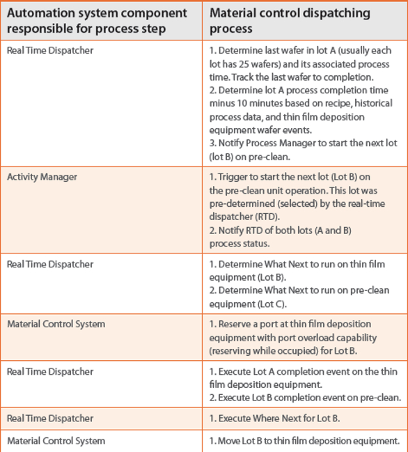
Figure 3 shows an example of an automated scheduling strategy build using an icon based, drag-and-drop programming approach. These rule based strategies are typically developed by semiconductor industrial engineers and can calculate optimal scheduling routes in real-time, taking in consideration asset state, asset performance, material availability and business needs.
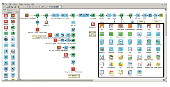 Figure 3. Typical icon based strategy to optimize semiconductor scheduling operations in real-time.
Fault Detection and Classification
Excursion detection and failure mode determination, called Fault Detection and Classification or “FDC” in the semiconductor industry, is employed on virtually all semiconductor processes.25,26 FDC combines real-time trace data collection of key equipment and process variables, along with process output quality information and advanced analytics such Principal Component Analysis (PCA) to determine when an excursion has occurred. These excursions can be indicative of a process change that might impact product quality or an equipment system change that might relate to equipment or equipment component health. Acting on these FDC indications has translated to benefits such as improved product quality, reduced product scrap and reduced downtime.
Virtual Metrology
Virtual metrology (a.k.a soft sensing) is used during semiconductor manufacturing to model and predict equipment and product quality parameters.16-18 These predictions are used in semiconductor manufacturing to detect, and control, quality excursions and equipment and component health issues without increasing process cycle time. Thus virtual metrology is often employed in critical processes in the process flow, where process control and cycle time have significant impact on the overall production yield and throughput. Some predictive algorithms and methods used in the semiconductor industry for virtual metrology are Partial Least Squares, Support Vector Machines, Multiple Linear Regression, Artificial Neural Networks and ensemble methods.
Predictive Maintenance
Predictive Maintenance, PdM, also referred to as Predictive Preventative Maintenance (PPM) or a component of Prognostics and Health Management (PHM) is receiving considerable attention in semiconductor manufacturing because it is focused on reducing unscheduled downtime, which is a major source of quality loss and cost in manufacturing.17,27,28 While some PdM solutions are relatively straight-forward extensions of FDC, most involve extensive data mining and analysis capabilities to develop models that not only predict the future occurrence of an equipment or component failure, but also indicate the time horizon for remaining useful time as well as a confidence and range of the prediction.27 These PdM prediction events are linked into maintenance, inventory, scheduling and manufacturing execution systems to optimize uptime, cost, productivity and quality. PdM could play a fundamental role within any plant Lean Manufacturing initiative since it de-risks the process and allows for the time horizon to be factored in during preventive maintenance optimization calculations, thus reducing planned downtime as well. Figure 4 shows an example of a PdM application deployed in semiconductor manufacturing. In this PdM application a multivariate failure mode model was used to estimate a PdM index that triggers an alarm when heating devices (lamps in this case) need to be replaced. Before the implementation of this PdM strategy, the user either ran the lamps to failure, resulting in unscheduled downtime and scrap, or used simple fault detection techniques to detect imminent failure (~4 hours in advance). The imminent failure region in the depicted PdM index curve is marked in red. When operating in this red region there is a high risk of unscheduled downtime, scrap and low yield. With this PdM index model the plant was able to predict failures ~ 5 days in advanced (yellow region). This longer time-to-fail horizon allows the plant to optimize the maintenance schedule. The prediction accuracy of this failure mode model is over 80%.
 Figure 4. A PdM index was calculated using multivariate data analysis for lamps used as radiation source during a gas deposition process. The health of the lamps impacts the product quality. A plot of this health index (PdM) is shown above. Operating at lower PdM index regions (blue and yellow traces) is safe whereas operating at a high PdM index (red trace) is risky and can impact yield and productivity.
A sample of actual reported benefits from application of these advanced technologies in semiconductor manufacturing operations is provided in Table 3. Many of the benefits arise from the combination of these technologies in a complementary fashion and the integration of the capabilities with existing system for manufacturing execution, scheduling and maintenance.
Table 3. Sample of reported benefits from application of advanced diagnostics and control capabilities in semiconductor manufacturing (data supplied by Applied Materials)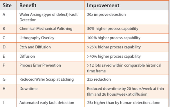
Semiconductor Operational Excellence Journey
The semiconductor industry’s journey towards innovation and operational excellence has been long (over thirty years) and as aforementioned market driven. Given the complexity of the semiconductor chip manufacturing process, this journey has also relied on systematic methodologies such as Six Sigma, Lean Manufacturing and continuous improvement combined with the adoption of advanced data analytics (univariate statistical process control and multivariate modeling), process technologies (e.g. double patterning lithography) and advanced sensing (e.g. spectroscopy, reflectometry and residual gas analysis). Proper and timely data analytics have been key in enabling OpEx and continuous improvements in this industry. In semiconductor manufacturing it is not common to perform process improvements without baseline analytics to determine process control ranges (or the lack of them), which follows continuous improvement and often six sigma precepts. Figure 5 shows a timeline of some of the advances and innovation incorporation in semiconductor manufacturing from 1993 to 2012.
 Figure 5. Timeline of Advances in Semiconductor Manufacturing.
Leveraging Lessons from Semiconductor for Pharma
The pharmaceutical industry has the opportunity of leveraging many lessons from Silicon Valley to ensure a smooth transition to the cyberphysical and decentralized decision era. The first, and most important lesson, is the criticality of IT infrastructure integration. Integration of the process components and IT infrastructure needs to be achieved in order to comprehensively optimize the performance of a process with real-time control and intelligent decision making based on raw material properties, process health and business needs.
Vertical networking of production systems to enable smart factories/ plants is still at a very early stage within the pharmaceutical industry especially when operating in batch mode. In many pharmaceutical plants we can still find a very fragmented IT infrastructure, which doesn’t allow generating a comprehensive picture of the process state, let alone making holistic data driven decisions in real-time. Making data and context available with real-time data infrastructure solutions will be the key enabler for integration and data-driven decision making. Even though many pharma companies are embracing real-time data infrastructure solutions, advanced data analytics and machine learning algorithms are not commonly incorporated within operations and/or planning control strate-gies yet.
The use of integrated real-time data infrastructures is of paramount importance when developing and implementing supervised data-driven models using machine learning approaches. In many pharmaceutical plants, process or equipment fault context, product quality data, maintenance logs and timely process information doesn’t reside within the same database. Thus, in order to identify fault models or any other soft model type such as those used for PdM, significant efforts in offline data identification, retrieval and merging has to be performed prior to modeling. These efforts are further complicated when process changes are implemented, as they may invalidate some empirical models. Thus, a continuous automated learning or algorithm training approach is recommended in order to develop less cumbersome life cycle model maintenance practices for data driven approaches. This approach is only realistically possible using integration, aggregation and evolutionary automated (or semi-automated) modeling practices.
 Figure 6. Vertical networking of production systems to make holistic and intelligent data-driven decisions.
Summary
The Industry 4.0 concept is the expected evolutionary path for all manufacturing arenas. The semiconductor industry has been forced to adopt many of the pillars of Industry 4.0 and Advanced Manufacturing in order to survive and thrive in the markets, and to adjust to technology demands. Semiconductor manufacturing processes are highly complex and sophisticated and yet the manufacturing metrics from this industry are significantly higher than the ones produced by pharma. This should be regarded by the pharmaceutical industry as a tremendous opportunity to leverage innovative technologies that are already mature in other industries and have been proven to improve the effectiveness and efficiency of highly complex operations. Leveraging lessons learned from the semiconductor journey should greatly benefit the pharmaceutical industry and our health care system while minimizing the cost and risk associated with early adoption.
 References
- FDA, Pharmaceutical cGMPs for the 21st Century —A risk-based approach final report. 2004.
- Davenport, T.H. and J. Dyché, Big Data in Big Companies. 2013, SAS Institute Inc.
- Editors, FDA Approves Tablet Production on Janssen Continuous Manufacturing Line, in Pharmaceutical Technology. 2016.
- Moretto, J., et al., Process Raman Spectroscopy for In-Line CHO Cell Culture Monitoring. American Pharmaceutical Review, 2011. 14(3): p. 18-25.
- Rathore, A.S., et al., Applications of Multivariate Data Analysis in Biotech Processing. BioPharm International, 2007. 20(10).
- Yu, L. Continuous Manufacturing Has a Strong Impact on Drug Quality. FDA Voice 2016; Available from: http://blogs.fda.gov/fdavoice/index.php/2016/04/ continuous-manufacturing-has-a-strong-impact-ondrug-quality/.
- Smart America. 2016; Available from: http:// smartamerica.org/about/.
- Schlaepfer, R.C. and M. Korsch, Challenges and solutions for the digital transformation and use of exponential technologies. 2015, Deloitte.
- Undey, C., et al., Process Analytics Experiences In Biopharmaceutical Manufacturing. European Pharmaceutical Review, 2012. 17(3): p. 22-29.
- Garguilo, L., Silicon Valley Meet BioPharma and its CMOs (Please). Outsourced Pharma, 2016.
- Maslaton, R., The Semiconductor Industry: A Role Model for the Pharmaceutical Industry? Pharmaceutical Technology, 2005. 29(11).
- Stamatis, D.H., The OEE Primer: Understanding Overall Equipment Effectiveness, Reliability, and Maintainability. 2010: CRC Press.
- Sze, S.M. and M.-K. Lee, Semiconductor Devices: Physics and Technology 3rd Edition. 2010: John Wiley and Sons
- Gupta, J.N.D., et al., Operational Planning and Control of Semiconductor Wafer Production. Production Planning & Control 2006. 17(7): p. 639–647.
- International Technology Roadmap for Semiconductors (ITRS): Factory Integration Chapter. 2015, International Roadmap Committee 2.5.
- Aftab Khan, J.M.a.D.T., Fab-wide Control Utilizing Virtual Metrology,” (invited) IEEE Trans. on Semiconductor Manufacturing-Special Issue Advanced Process Control, 2007: p. 364-375.
- G. Roeder, M.P., M. Schellenberger, R. Öchsner, L. Pfitzner Application of virtual metrology and predictive maintenance in semiconductor manufacturing, in SEMICON Europa2010 – TechARENA -Automation and Process Control Session. 2010: Dresden, Germany.
- Pilsung Kanga, D.K., Hyoung-joo Leeb, Seungyong Dohc, , Sungzoon Choa, Virtual metrology for run-to-run control in semiconductor manufacturing. Expert Systems with Applications, 2011. 38(3).
- Chiang, T.C., et al., Real-time Dispatch Gets Real-Time Results in AMD’s Fab 25, in IEEE/ SEMI Advanced Semiconductor Manufacturing Conference and Workshop ASMC 97 Proceedings, 1997
- Zhang, H., Z. Jiang, and C. Guo, Simulation-based optimization of dispatching rules for semiconductor wafer fabrication system scheduling by the response surface methodology. The International Journal of Advanced Manufacturing Technology, 2009. 41(1): p. 110-121.
- Chung, B.s., et al., Setup Change Scheduling for Semiconductor Packaging Facilities Using a Genetic Algorithm With an Operator Recommender. IEEE Transactions on Semiconductor Manufacturing, 2014. 27(3): p. 377-387.
- Lee, S. and J. Ni, Genetic Algorithm for Job Scheduling with Maintenance Consideration in Semiconductor Manufacturing Process. Mathematical Problems in Engineering, 2012. 2012: p. 1-16.
- Uzsoy, R., C.-Y. Lee, and L.A. Martin-Vega, A Review of Production Planning and Scheduling Models in The Semiconductor Industry Part I: System Characteristics, Performance Evaluation and Production Planning. IIE Transactions,, 1992. 24(4): p. 47-60.
- Ni, Y., et al., Development of an Integrated Real Time Dispatching System: A Case Study at a Semiconductor Assembly and Test Factory. Journal of Manufacturing Technology Management, 2014. 25(7): p. 980-997.
- Agrawal, G.K., S.Y. Loh, and A.B. Shebi. Advanced Process Control (APC) and Real Time Dispatch (RTD) system integration for etch depth control process in 300mm Fab. in 2015 26th Annual SEMI Advanced Semiconductor Manufacturing Conference (ASMC). 2015. IEEE.
- Chen-Fu Chien, C.-Y.H., Pei-Nong Chen Semiconductor fault detection and classification for yield enhancement and manufacturing intelligence. Flexible Services and Manufacturing Journal, 2013. 25(3): p. 367-388.
- Goodlin, B.E., et al., Simultaneous Fault Detection And Classification For Semiconductor Manufacturing Tools, in Meeting of the Electrochemical Society, International Symposium on Plasma Processing XIV, Abs 413. 2002: Philadelphia.
- J. Iskandar, J.M., K. Subrahmanyam, P. Hawkins and M. Armacost Predictive Maintenance in Semiconductor Manufacturing: Moving to Fab-Wide Solutions. in 26th Annual Advanced Semiconductor Manufacturing Conference (ASMC 2015). 2015. Saratoga Springs, New York.
- James Moyne, M.A., The Move To Big Data And Predictive Analytics In Semiconductor Manufacturing. Nanochip Fab Solutions, 2014. 9(2).
Author Biographies
Saly Romero-Torres has over 15 years of experience in the field of process analytical technology and advanced manufacturing of bio-pharmaceuticals. She obtained a Ph.D. in 2006 from Purdue University in the area of advanced pharmaceutical process analysis and has worked for pharmaceutical companies such as Schering Plough, Wyeth and Pfizer. While at the industry, she developed many best practices for the implementation of advanced process analytics. In 2014 Dr. Romero-Torres founded Bio-Hyperplane LLC, a data analytics and pharmaceutical consultation company.

James Moyne has over 20 years of experience in the area of advance controls and manufacturing systems for semiconductor manufacturing. He obtained his Ph.D. in Engineering from University of Michigan in 1990, where is a faculty member. He is also a Technology Specialist at Applied Materials and founder of MiTeX Solution, Inc. in 1993, which provided the first Advanced Process Control solutions for the Semiconductor industry. James’ research interests include predictive technologies, big data, model-based process control, real-virtual environment fusion, and renewal energy “grid” networks and diagnosis.

Madhav Kidambi has over 15 years of experience in the area of Industrial and Systems Engineering. In 2000 he obtained an MS degree in engineering from the Virginia Polytechnic Institute and State University. Madhav currently works for Applied Materials as Global Product Manager for Productivity Solutions. Madhav expertise resides in optimization and automation of Scheduling and Dispatching as well as Six Sigma continuous improvement.