While Near-Infrared Spectroscopy (NIRS) has been used in the pharmaceutical industry since the 1980s, it continues to evolve today. When I first investigated NIRS as a technique, most instruments used were UV/Vis with and “also scans in the NIR” option. Two large (relatively) companies, Pacific-Scientific (later NIRSystems) and Technicon (later Bran+Leubbe), were selling delicate NIR instruments (bench-top). Both were good (for the era, c. 1983), but software was both limited and non-GMP.
The earliest serious work performed on equipment designed as a NIR spectrometer was for agriculture (grain, tobacco, meat) and fabrics. Only after we proved its value for pharmaceuticals (1980’s), did the instrument companies begin to write CFR-compliant software and design a myriad of specialty instruments (process, hand-held, miniature) and interfaces for the pharmaceutical and biopharmaceutical industries.
The “norm” for NIT instruments through the early 1990’s was a tungsten-halogen lamp, a grating or filters, and lead sulphide (PbS) detectors. Most measurements took 10-30 seconds; good for lab work and containers in a warehouse, but not for real-time analyses in production. Pfizer built the closest thing to process analysis (PAT?) by constructing a booth between two process lines, sampling over the course of the process, running NIR (transmission) analyses, and keeping a “running score” of the content uniformity. This technique was approved as the first “real-time” release program by the FDA. More rapid instruments were still too expensive, mainly due to the competition for indium-gallium-arsenide (InGaAs) for fast, lownoise detectors.
With the collapse of telecom industry came an abundance of InGaAs detectors. There are used to relay voice and data in fiber optic cables (on land and under water) with almost no loss of power or information. Prior to 1992, a diode-array detector of InGaAs could cost $10,000 or more; thus, too large for a relatively new (to pharma) technology. As the price dropped precipitously, any instrument company was free to employ them. When cooled, the wavelength range, speed of response, and noise levels are superior to the PbS (lead sulfide) detectors, used for decades.
Today, new NIR instruments follow the credo, “smaller, faster, and less expensive.” Add to that “sturdier, quieter, and user-friendly,” and we see why there is a huge wave of interest in NIRS, particularly for PAT/QbD (Process Analytical Technology/Quality by Design) applications. All these improvements make the instruments perfect for continuous manufacturing, as well. Several smaller instruments have existed for decades, (acousto-optic tunable filters, linear variable filters, and diode arrays), but each had limits (resolution, speed, cost), so we needed more. What are some of the improvements, innovations, and software updates?
MEMS: Or Micro-Electro Mechanical Systems, are made up of components between 1 and 100 micrometers in size. The actual devices (the wavelength selection portion) generally range in size from 20 micrometers to a millimeter, but components in arrays (digital micromirror devices) can be more than 1000 mm2 . They consist of a microprocessor and several components, interacting with the surroundings as microsensors. Due to the large surface to volume ratio of MEMS, ambient forces can be more important for design considerations than larger, mechanical devices (gratings, Fourier Transform’s). MEMS are fabricated by using modified semiconductor device fabrication technologies, normally used for electronics, including molding and plating, wet and dry etching, electro-discharge machining, and other technologies capable of manufacturing small devices. An early example of a MEMS device is called the “resonistor,” an electromechanical monolithic resonator and the resonant gate transistor.
Developed as Fabray-Perot interferometers for communications relays, MEMS were converted to spectroscopy when the telecom market contracted. Initially, the units addressed the portable and rugged categories for portable instruments, but failed the “inexpensive” criterion. However, recent advances in the construction, notably by companies such as SiWare (Cairo, Egypt) have caused costs of instruments to plummet. The above-mentioned company has developed MEMS interferometers on silicon chips, such that they may be had for “pocket-change.” They have also developed multiple MEMS chips on a single card, capable of working in unison, providing a greater throughput of light for commercial applications.
Another producer of MEMS-based equipment is Spectral Engines (Oulu, Finland: Figure 1). The sensor (named NIRONE) uses a patented MEMS Fabry-Perot Interferometer, a fully programmable optical filter. The sensor can be driven across the whole wavelength range or can operate only at selected wavelengths (hopping). The sensor’s algorithms replace temperature stabilization. It uses a single point detector in lieu of a linear array, making it very inexpensive.
 Figure 1. Spectral Engines NIR Unit
The use of a single detector and Fabry-Perot Interferometer technology allows the use of a larger detector area than linear arrays where the light is restricted by a slit, making the unit’s S/N ratio significantly better. The single InGaAs detector provides better sensitivity and specificity in material sensing applications.
Three wavelength ranges are: 1350 – 1650 nm (14-18 nm resolution), 1550 – 1950 nm (16-22 nm resolution), 1750 – 2150 nm 20-26 nm resolution). Allowing a choice of resolution vs. speed. Two tungsten vacuum lamps are sources (bulb life: > 40,000 hours) for continuous use, without frequent maintenance. Size (W x L x H) 25 x 25 x 17.5 mm3 ; Weight: 15 g
DLP® Technology: For numerous, current applications, expensive, lab-based spectrometers are required for quantitative and qualitative analyses. Pharmaceutical and biopharmaceutical applications benefit from in-line/at-line portable equipment to perform real-time material analysis. The digital micromirror device (DMD) is a highly efficient spatial light modulator that can enable compact spectrometers to meet these requirements (see Figure 2). Initially developed by Texas Instruments for projectors (from PowerPoint presentations to stadium scoreboards), the basis of operation is an array of micro-mirrors, the angle(s) of which determine the wavelength (color or NIR spectrum). They can be electronically controlled such that multiple units may be made into clones, giving identical spectra. This obviates the need to use math algorithms to message a spectrum from one NIR instrument to resemble a spectrum on the instrument used to generate the Chemometric equation.
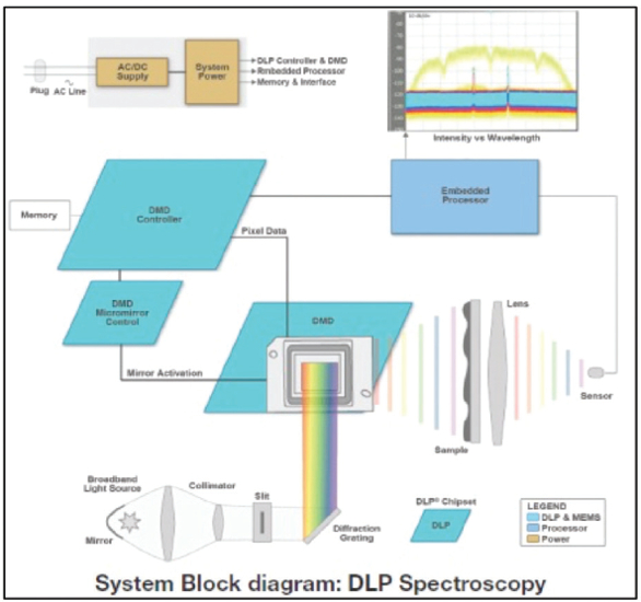 Figure 2. System Block Diagram for DLP Spectroscopy
Mechanically robust, rugged designs are made possible by eliminating (conventional) moving mirrors or gratings. A digital switching device, the DMD delivers constant results over time and temperature (see Figure 3). It has high speed wavelength selection and filtering, and allows method developers to attenuate individual wavelengths. Spectrometers based on the DMD can be easily programmed for multiple materials, creating flexible optical engine designs to satisfy the demands from multiple applications. Pattern rates up to 32 kHz with optical switching speeds of ~2μs obtain high speed and precise full spectrum scan data. Real-time data acquisition for applications such as inline inspection.
 Figure 3. Neolitics new DLP-Based NIR Process Spectrometer. Incident NIR, detector port, vision lens.
They are optically efficient from 365nm to 2500nm (Supports UV, VIS and NIR spectrometers). One of the newest devices, designed for GMP (and 21CFR11) process analysis and control was introduced by a new company (Neolitics) at PittCon this year (Figure 3). Primarily built for the NIR region, it also has a “vision” lens to assure visual confirmation of what is being analyzed. The instrument was designed with an interesting geometry. “Traditional” NIR reflection-type instruments have a 00 – 450 illumination-collection configuration. That is, the light illuminated the sample “normally” or perpendicular (00 ) and the detectors placed at a 450 angle, above the sample. By illuminating at 450 and collecting at 00 , a larger portion of specular (simple reflected, non-absorbed) light is avoided, enhancing the s/n ratio to 25,000, according to the company.
At PittCon, Neolitics introduced a new class of NIR spectrometer specifically for in-line industrial process control to be deployed within any production environment no matter how space limited the installation or harsh the environment. Their instrument is a solid-state device with no moving parts making it compact and rugged. It was originally used to go downhole for oil and gas exploration. Thus, it had to be capable of operating over extreme changes in environmental conditions without drift or calibration error.
The company developed and patented a spectrometer utilizing an adaptive optical element to eliminate drift. The optical element they use is Texas Instrument’s Digital Light Processor (DLP™). The DLP™ revolutionized the television industry by enabling the development of large screen rear projection televisions that could fit in your living room. Over decades of commercial applications, the adaptive optical element at the core of the Neolitics’ first product is mature and moreover, is still being improved due to the success of the personal projectors that utilize the DLP™.
The company is calling their first product DNIRA™, which stands for Distributable Near-InfraRed Analyzer (7 kg, 9.5”x 6.5” x 8”). They are trying to deliver two messages with the name: 1) the device is easy to deploy, so clients will DISTRIBUTE them throughout their processes, and 2) clients will map the unique DNA of their processes.
The DLP™ routes the light both spectrally and spatially inside the spectrometer. Spatial routing allows it to reference the internal state (due to source aging or environmental changes) while continuously measuring the sample under test. This routing allows them to eliminate drift within each spectral band, the primary reason NIR spectrometers require maintenance (i.e., recalibration). Spectral routing affords them multiple advantages, specifically: 1) it allows for the utilization of a single element photodiode as opposed to a diode array, enabling signal-to-noise ratios exceeding 35,000:1 across most of the spectral range (1300 nm - 2600 nm); 2) it allows methods that have previously inaccessible to NIR spectrometers; and 3) it allows for instrument cloning. Note that the device’s ability to internally reference each spectral channel independently is critical to eliminating the routine maintenance (i.e., recalibration requirement) of traditional NIR instrumentation.
SR enables three key functions, it allows: 1) use of a single element photodiode vs. a diode array, enabling a S/N >35,000:1 across most of the spectral range (1300 nm-2600 nm); 2) new spectral methods, previously inaccessible to NIR instruments; and 3) in combination with spatial routing, it allows for instrument cloning.
Currently, instrument manufacturers cannot mass produce analyzers that are spectrally equivalent (i.e., clones). For a device to be spectrally equivalent, every spectral band within the instrument must have identical spectral bandwidth in addition to identical throughput. If they deliver on their promises, they will be the first optical analyzer company able to provide clients with true “hotswappable spares”. Their ability to provide hot-swappable spares will allow them to effectively eliminate method transfer, which they believe has been the bane of NIR analysis since its inception and the primary factor that has limited the transitioning of NIR from the laboratory to in-line installations.
This technology could eliminate the need for service technicians with their warranty program. An annual maintenance or warranty package will provide a second instrument (a clone of the first instrument). In theory, waiting for a service technician will disappear, allowing for no process down time. The goal is to enable the client to install the instrument in under 30 minutes in the event of an outage, after which the client ships the down unit to a service repair center. While not exactly “maintenance free,” it is relatively close, compared with what is done today.
If this equipment is as good as claimed, it should be impressive. Hyperspectral Imaging (HIS): Several companies developed chemical imaging instruments, introducing them with the new millennium. Two major approaches were used: a scanning array and a planer array (of InGaAs diodes). A resulting Hyperspectral Chemical Image showed both the materials in a solid/powder sample and their special relationships (homogeneity, particle agglomeration, etc.) as seen in Figure 4.
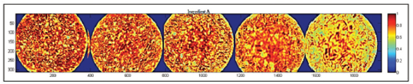 Figure 4. (False-color, RGB) Hyperspectral Images of Tablets, showing the homogeneity of API (these images may be taken through polymer packaging)
The current, best-established imaging technology for imaging is the “push-broom” approach, developed by VTT (Oulu, Finland). There are several vendors of the technology, worldwide (VTT only licenses its technology). The hand-held device, made by Specim, is shown in Figure 5. At 207 x 91 x 74 mm (depth with lens 125.5 mm), it is quite easily transported. It has a Vis/SW-NIR Wavelength range (400 – 1000 nm). Its Viewfinder camera is a 5 Mpixel (Up to 32 GB SD memory card). I t has a display & keyboard 4.3” touch screen and is connected via USB connector - Type-C and only weighs 1.3 kg.
 Figure 5. Hand-Held Hyperspectral Imaging Camera (HIC)
A more complex, process instrument is available for PAT/QbD applications. The device by Indatech (Clapiers, FR), incorporates the push-broom technology, equipped with fiber optics to perform realtime analyses (See Figure 6, multi-fiber probe head). The pattern of light returned through the multiple fibers (it is illuminated at the center) allows for both qualitative and quantitative analyses at (up to) 200,000 units/hour. These applications include in-process steps (blending, granulating) and final products (capsules, tablets, vials: see Figure 7).
 Figure 6. Indatech Push-Broom HIS fi ber probe
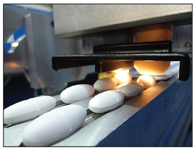 Figure 7. Hyperspectral Imaging Spectra of tablets, in real time.
Closing Remarks
A simple article cannot convey the giant (pun intended) steps that we have taken on miniature NIR instruments. I would strongly suggest perusing the aisles of your next professional conference (IFPAC, Analytica, etc.) and see, touch, and see demos of all the wonderous instruments available for pharmaceutical and biopharmaceutical applications.
Emil W. Ciurczak is a respected consultant and author on spectroscopy topics. Mr. Ciurczak attends all major spectroscopy conferences looking for the latest technologies. This article is an overview of some of the latest breakthroughs in spectroscopic instrumentation. Companies and products mentioned in this article are not an endorsement by American Pharmaceutical Review. Opinions are those of the author.